
EEPROM History and the Evolution of Non-Volatile Memory
The development of non-volatile memory—storage that retains data even when power is removed—was a pivotal journey in semiconductor engineering. Before the ubiquity of modern storage, researchers in the 1970s raced to create memories that could be electrically re-programmed, moving away from the limitations of early read-only options.
Early Attempts at Electrically Re-programmable Memory
The early 1970s saw a surge of experimentation across global research institutes and corporations. In 1971, Yasuo Tarui, Yutaka Hayashi, and Kiyoko Nagai of the Electrotechnical Laboratory in Japan presented early research on electrically re-programmable non-volatile memory. While they successfully fabricated a device in 1972, their design relied on capacitors, a characteristic absent in modern Electrically Erasable Programmable Read-Only Memory (EEPROM).
Parallel efforts emerged in the corporate sector. IBM patented a re-programmable non-volatile memory in 1972, the same year Fujio Masuoka at Toshiba patented an avalanche injection type MOS (Metal-Oxide-Semiconductor). By 1974, NEC patented an electrically erasable carrier injection device, eventually securing the "EEPROM®" trademark in 1978.
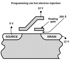
These early devices relied on avalanche hot-carrier injection, a process where high-energy electrons are injected into a storage layer. However, these first-generation memories struggled with reliability, specifically regarding data retention periods and the limited number of erase/write cycles they could endure.
During this era, nearly every major semiconductor player was involved in the race, including Toshiba, Sanyo, IBM, Intel, NEC, Philips, Siemens, Honeywell, and Texas Instruments.
The Transition to Modern EEPROM
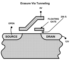
The shift toward modern EEPROM began with the introduction of Fowler-Nordheim tunnelling, a quantum mechanical process that allows electrons to pass through a thin insulating barrier. This method was first used to erase data in a device invented by Bernward and patented by Siemens in 1974.
A major breakthrough occurred in February 1977 when Eliyahou Harari of the Hughes Aircraft Company patented a technology utilizing Fowler-Nordheim tunnelling through a thin silicon dioxide layer situated between the wafer and the floating-gate. This architecture became the foundation for the modern EEPROM devices produced by Hughes.
By May 1977, further advancements were disclosed by Fairchild and Siemens. Fairchild utilized a SONOS (polysilicon-oxynitride-nitride-oxide-silicon) structure with a silicon dioxide layer thinner than 30 Å (Angstroms, where 1 Å = 10-10 m), while Siemens employed a SIMOS (stacked-gate injection MOS) structure to facilitate tunnelling hot-carrier injection.
The Intel FLOTOX Innovation
Between 1976 and 1978, an Intel team led by George Perlegos refined tunnelling EPROM technology. In 1978, they produced the Intel 2816 chip, a 16K (2K word × 8) bit memory featuring a silicon dioxide layer thinner than 200 Å. This structure, publicly introduced in 1980 as FLOTOX (floating gate tunnel oxide), significantly boosted reliability, allowing up to 10,000 erase/write cycles per byte.
Despite its durability, FLOTOX required a high VPP bias voltage of 20–22V for byte erasure, though read operations remained at 5V. This challenge led George Perlegos and two colleagues to leave Intel in 1981 to form Seeq Technology, which developed on-device charge pumps to generate the necessary high voltages internally. Seeq Technology was later acquired by Atmel, a company founded by Perlegos in 1984.
EAROM: A Specialized Variant
Another evolution in this field is Electrically Alterable Read-Only Memory (EAROM). Unlike standard EEPROM, EAROM is designed to be modified one or a few bits at a time. Because the writing process is very slow and typically requires a higher voltage (around 12V) than read access, EAROMs are best suited for applications requiring only infrequent and partial rewriting.
Key Facts
- First EEPROM Trademark: Applied for by NEC in 1975 and granted in 1978.
- Core Mechanism: Modern EEPROM relies on Fowler-Nordheim tunnelling through a thin silicon dioxide layer.
- FLOTOX Impact: Increased erase/write cycle endurance to 10,000 times per byte.
- Voltage Requirements: Early FLOTOX required 20–22V for erasing, leading to the invention of on-device charge pumps.
- SONOS Structure: Utilizes a silicon dioxide layer of less than 30 Å.
| Technology | Primary Mechanism | Key Characteristic | Notable Developer |
|---|---|---|---|
| Early 1970s Memory | Capacitors / Avalanche Injection | Low reliability/endurance | Electrotechnical Laboratory |
| Modern EEPROM | Fowler-Nordheim Tunnelling | Thin silicon dioxide layer | Hughes Aircraft Company |
| FLOTOX | Floating Gate Tunnel Oxide | 10,000 cycle endurance | Intel |
| EAROM | Bit-level alteration | Slow write, high voltage (12V) | Various |
Frequently Asked Questions
What is the difference between early re-programmable memory and modern EEPROM?
Early attempts in the 1970s often relied on capacitors or avalanche hot-carrier injection, which suffered from poor data retention and low endurance. Modern EEPROM uses Fowler-Nordheim tunnelling through a thin silicon dioxide layer for better reliability.
What was the significance of the FLOTOX structure?
Introduced by Intel, FLOTOX (floating gate tunnel oxide) improved the endurance of the memory, allowing it to be erased and rewritten up to 10,000 times per byte.
Why were charge pumps necessary for EPROMs?
Because devices like FLOTOX required high voltages (20–22V) for erasing data—far higher than the 5V used for reading—charge pumps were developed to generate these high voltages directly on the device.
What is EAROM and when is it used?
Electrically Alterable Read-Only Memory (EAROM) is a type of EEPROM that allows for the modification of a few bits at a time. It is used in applications where rewriting is infrequent and only partial updates are needed.
What does SONOS stand for in memory architecture?
SONOS stands for polysilicon-oxynitride-nitride-oxide-silicon, a structure used by Fairchild to implement Fowler-Nordheim tunnelling with a very thin silicon dioxide layer (less than 30 Å).