
Pentium Processors: The Evolution of Intel's Iconic CPU Brand
The Pentium brand represents one of the most enduring names in computing history. Launched by Intel in the early 1990s, the Pentium line transitioned from being the flagship high-performance processor for consumers to a reliable entry-level option. This evolution spans several microarchitectures, shifting from the early superscalar designs to the modern multi-core efficiency of the Core era.
The P5 Microarchitecture: The Original Pentium
Introduced in 1993, the original P5 microarchitecture was a superscalar follow-on to the 80486 processor. A superscalar processor is one that can execute more than one instruction per clock cycle. This era saw the introduction of the Pentium MMX, and some versions were released as Pentium OverDrive to allow users to upgrade older CPU sockets.
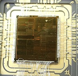
The P5 line evolved through several iterations, reducing the process size from 0.8 μm to 0.25 μm, which allowed for higher clock speeds and increased L1 cache (the smallest, fastest memory located closest to the CPU core).
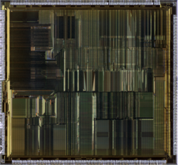
P5 Generation Specifications
| Core | Process | Clock Rates | L1 Cache | Socket | Release Date |
|---|---|---|---|---|---|
| P5 | 0.8 μm | 60–66 MHz | 16 KB | Socket 4 | March 1993 |
| P54C | 0.6 μm | 75–120 MHz | 16 KB | Socket 5 | October 1994 |
| P54CS | 0.35 μm | 133–200 MHz | 16 KB | Socket 7 | June 1995 |
| P55C | 0.35 μm | 120–233 MHz | 32 KB | Socket 7 | January 1997 |
| Tillamook | 0.25 μm | 166–300 MHz | 32 KB | Socket 7 | August 1997 |
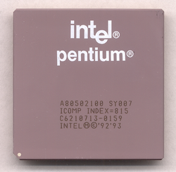
The P6 Microarchitecture: Pro, II, and III
In 1995, Intel introduced the P6 microarchitecture, debuting with the Pentium Pro. This architecture was a significant leap forward, introducing out-of-order execution—a technique where the CPU processes instructions as resources become available rather than in the strict order of the program—and an integrated second-level (L2) cache.
The P6 lineage expanded into the Pentium II and Pentium III. The Pentium II introduced MMX instructions and shifted from sockets to Slot 1. The Pentium III further refined this, eventually moving back to Socket 370. During this time, Intel introduced the Celeron brand for budget-friendly versions with reduced features, such as smaller caches.
NetBurst and the Pentium 4 Era
Launched in 2000, the NetBurst microarchitecture focused on achieving very high clock frequencies through a much longer pipeline. This era was defined by the Pentium 4. For enthusiasts, Intel released the Pentium 4 Extreme Edition.
NetBurst also led to the first multi-core Pentium: the Pentium D. Unlike later designs, the Pentium D integrated two separate Pentium 4 chips into a single package to achieve dual-core performance.
The Shift to Pentium M and Core Microarchitecture
In 2003, Intel pivoted back to the P6 design for mobile devices, creating the Pentium M. This processor was significantly more power-efficient than the Mobile Pentium 4. The dual-core version of this design, codenamed Yonah, was marketed as both Core Duo and Pentium Dual-Core.
This transition marked a branding shift: the "Core" brand became the mainstream flagship, while "Pentium" was repositioned as a mid-to-low-end tier between Celeron and Core. The Core microarchitecture eventually replaced all NetBurst-based processors.
Modern Pentium Iterations (2009–2021)
From 2009 onward, the Pentium brand continued through several architectural refreshes:
- Nehalem/Westmere: Introduced the Direct Media Interface (DMI), replacing the legacy Front-Side Bus (FSB).
- Sandy Bridge: Reintroduced Hyper-threading (allowing a single core to act as two logical processors) to the Pentium line.
- Ivy Bridge: The last Pentium processors to fully support Windows XP and Vista.
- Skylake: The final Pentium generation officially supported by Microsoft for versions of Windows earlier than Windows 10.
- Kaby Lake & Coffee Lake: Standardized Hyper-threading and integrated UHD Graphics.
- Comet Lake: The final major refresh, introducing the Pentium Gold series with 14 nm process technology.
Key Facts
- First Pentium: Launched in March 1993 based on the P5 microarchitecture.
- Architectural Shift: Moved from P5 to P6, then NetBurst, and finally to the Core microarchitecture.
- Multi-core Debut: The Pentium D was the first multi-core Pentium, using two chips in one package.
- Efficiency Pivot: The Pentium M (2003) returned to P6 roots to prioritize power efficiency over raw clock speed.
- Modern Branding: The "Pentium Gold" series represents the later stages of the brand's life in the Comet Lake era.
Frequently Asked Questions
What is the difference between Pentium and Celeron?
Historically, Celeron processors were low-end versions of Pentium processors, typically featuring a reduced feature set, such as smaller cache sizes or the absence of certain power management features.
What was the significance of the NetBurst microarchitecture?
NetBurst was designed to enable much higher clock frequencies than previous architectures by utilizing a longer instruction pipeline, though it was eventually superseded by the more efficient Core microarchitecture.
When did Pentium processors start supporting Hyper-threading?
While Hyper-threading existed in high-end Core i7 chips in 2008, it returned to the Pentium line with the Sandy Bridge microarchitecture in 2011 and again with the Kaby Lake G4560 in 2017.
Which Pentium processors support older versions of Windows?
Ivy Bridge models were the last to fully support Windows XP and Vista, while Skylake-based Pentiums were the last to be officially supported by Microsoft for versions earlier than Windows 10.
What is the Front-Side Bus (FSB) and what replaced it?
The FSB was the communication interface between the CPU and the system memory/chipset. It was replaced by the Direct Media Interface (DMI) starting with the Nehalem-based Pentium processors.